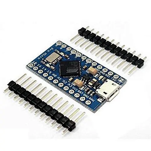
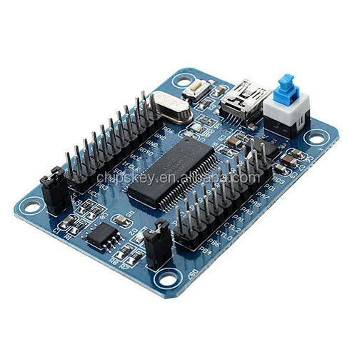
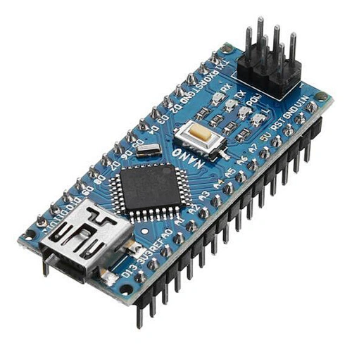
- Model Number:8017
- Place of Origin:Guangdong, China, USA
- Brand Name:Chipskey
- Lead Free Status:Lead free / RoHS Compliant
- Condition:Brand New With Original Manufacturer
- Packaging:Reel Tray Tube
- Maximum Operating Temperature:-40C ~ 125C
- Warranty:360days
- Operating Temperature:-40C ~ 125C
- Dissipation Power:1W-6W
- Application:Watch
- Supply Voltage:1.5V-6V
leaflabs Leaf maple
Description
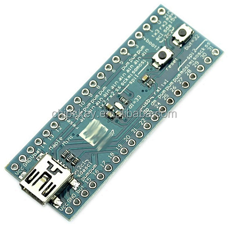
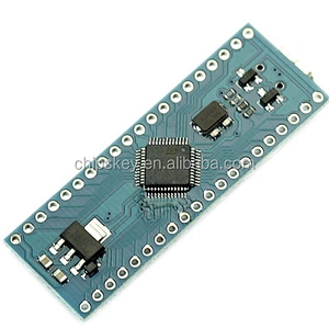
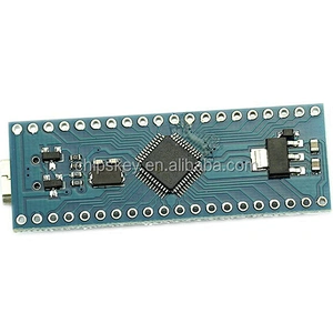
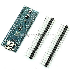
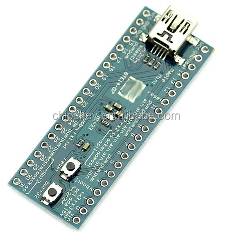
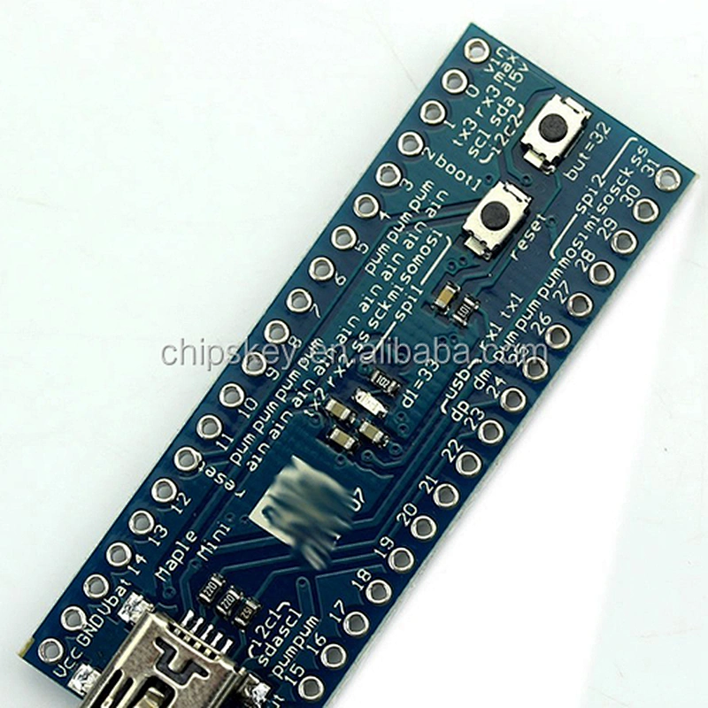
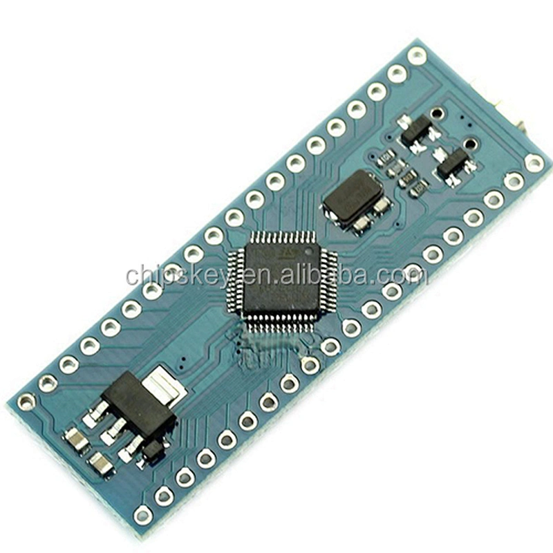
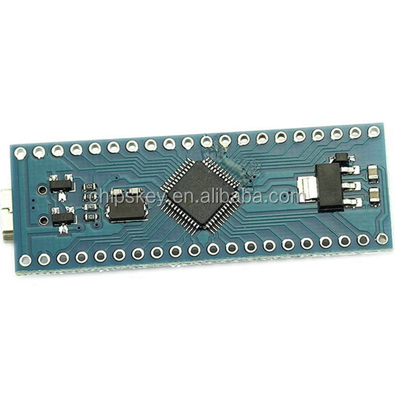
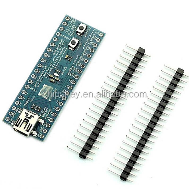
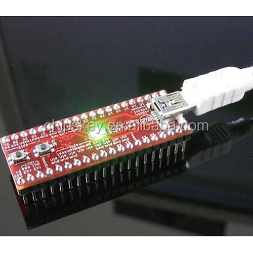
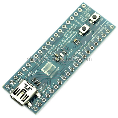
Maple Mini is a breadboard-able PCB for applications where space is limited or simply if a breadboard is the preferred prototyping tool. Smaller than a stick of gum, Maple Mini features a smaller, 48-pin STM32 with the same speed and memory as the original Maple, but 34 GPIOs. It can be powered by USB or an external supply. Maple Mini also maintains a complete silkscreen, making it uniquely detailed for a board its size.
- Dimensions: 2.02 x 0.72 inches
- Microprocessor: 32-bit Cortex M3 at 72MHz (STM32F103CBT6)
- Memory: 120 KB Flash and 20 KB SRAM
- I/O Pins: 34 (of which 12 provide PWM output at 16-bit resolution)
- ADCs: 9 (at 12-bit resolution)
- Peripherals: 4 timers, 2 I2Cs, 2 SPI ports, 3 USARTs
- Other: Sleep, stop, and standby modes; serial wire debug and JTAG interfaces
Techniques
Processor: STM32F103RCBT6, 32 Cortex-M3 processor
Frequency: 72 MHz
128 KB Flash and 20 KB SRAM
34 digital io ports (GPIOs)
12 16 precision PWM port
9 12 precision analog input (ADC) port
Two SPI channels
2 I2C channels
7-channel direct memory access (DMA) (dma.h)
3 USART (serial) channel
An enhanced and three general-purpose timers
Can be downloaded directly through the USB port and communications program
External JTAG
Nested Vectored Interrupt Controller (NVIC) (including external interrupt on GPIOs)
Support for low-power sleep mode and standard (<500 μA)
Operating voltage: 3.3 V
Input Voltage (recommended): 3 V - 12 V
Dimensions: 2.02"× 0.72"
Maple Mini powered
Can supply power to the Vin port or directly through the USB port.
GPIO information
Maple Mini has a total of 34 input / output pins, numbered from D0 to D33. Port and its neighboring Maple Mini label on the corresponding screen. However, they have some special uses by default.
The USB port D23 is D +, D24 is the USB D-. Such as their use as GPIO, then your program must first disable the USB port. But you know, disable USB serial bootloader means that priority will not work, you will need to pass Perpetual Bootloader for the next update.
D32 is the Mini button port port. Therefore, it is mainly used as an input port. When the key is pressed, the magnetic port will read high.
D33 is the Mini LED port port. Therefore, its main role is as an output port. When it was written with a high level, LED lights will be lit.
The main pin diagram
This table is based on the type of external pin for GPIO functions made available a summary."5V?"Column text indicates whether the pin is compatible with 5V level.
Note that this table does not detail, some pin additional features not listed.
| D0 | PB11 | | | 2_SDA | 3_RX | | Yes |
| D1 | PB10 | | | 2_SCL | 3_TX | | Yes |
| D2 | PB2 | | | | | | Yes |
| D3 | PB0 | CH8 | 3_CH3 | | | | |
| D4 | PA7 | CH7 | 3_CH2 | | | 1_MOSI | |
| D5 | PA6 | CH6 | 3_CH1 | | | 1_MISO | |
| D6 | PA5 | CH5 | | | | 1_SCK | |
| D7 | PA4 | CH4 | | | 2_CK | 1_NSS | |
| D8 | PA3 | CH3 | 2_CH4 | | 2_RX | | |
| D9 | PA2 | CH2 | 2_CH3 | | 2_TX | | |
| D10 | PA1 | CH1 | 2_CH2 | | 2_RTS | | |
| D11 | PA0 | CH0 | 2_CH1_ETR | | 2_CTS | | |
| D12 | PC15 | | | | | | |
| D13 | PC14 | | | | | | |
| D14 | PC13 | | | | | | |
| D15 | PB7 | | 4_CH2 | 1_SDA | | | Yes |
| D16 | PB6 | | 4_CH1 | 2_SCL | | | Yes |
| D17 | PB5 | | | 1_SMBA | | | |
| D18 | PB4 | | | | | | Yes |
| D19 | PB3 | | | | | | Yes |
| D20 | PA15 | | | | | | Yes |
| D21 | PA14 | | | | | | Yes |
| D22 | PA13 | | | | | | Yes |
| D23 | PA12 | | 1_ETR | | 1_RTS | | Yes |
| D24 | PA11 | | 1_CH4 | | 1_CTS | | Yes |
| D25 | PA10 | | 1_CH3 | | 1_RX | | Yes |
| D26 | PA9 | | 1_CH2 | | 1_TX | | Yes |
| D27 | PA8 | | 1_CH1 | | 1_CK | | Yes |
| D28 | PB15 | | | | | 2_MOSI | Yes |
| D29 | PB14 | | | | 3_RTS | 2_MISO | Yes |
| D30 | PB13 | | | | 3_CTS | 2_SCK | Yes |
| D31 | PB12 | | 1_BKIN | 2_SMBA | 3_CK | 2_NSS | Yes |
| D32 | PB8 | | 4_CH3 | | | | Yes |
| D33 | PB1 | CH9 | 3_CH4 | | | | |
GPIOAGPIOBGPIOC
|
| PA0: D11 | PB0: D3 | PC0: - |
| PA1: D10 | PB1: D33 | PC1: - |
| PA2: D9 | PB2: D2 | PC2: - |
| PA3: D8 | PB3: D19 | PC3: - |
| PA4: D7 | PB4: D18 | PC4: - |
| PA5: D6 | PB5: D17 | PC5: - |
| PA6: D5 | PB6: D16 | PC6: - |
| PA7: D4 | PB7: D15 | PC7: - |
| PA8: D27 | PB8: D32 | PC8: - |
| PA9: D26 | PB9: - | PC9: - |
| PA10: D25 | PB10: D1 | PC10: - |
| PA11: D24 | PB11: D0 | PC11: - |
| PA12: D23 | PB12: D31 | PC12: - |
| PA13: D22 | PB13: D30 | PC13: D14 |
| PA14: D21 | PB14: D29 | PC14: D13 |
| PA15: D20 | PB15: D28 | PC15: D12 |
The following table lists each port corresponds to a specific timer capture / compare channels.
TimerCh. 1Ch. 2Ch. 3Ch. 4
1 D27 D26 D25 D24
2 D11 D10 D9 D8
3 D5 D4 D3 D33
4 D16 D15 D32